- 您现在的位置:买卖IC网 > Sheet目录1200 > C8051F310DK-K (Silicon Laboratories Inc)DEV KIT FOR C8051F310/F311
�� �
�
�C8051F31x�
�4.5.� Serial� Interface� (J5)�
�A� RS232� transceiver� circuit� and� DB-9� (J5)� connector� are� provided� on� the� target� board� to� facilitate� serial� connec-�
�tions� to� UART0� of� the� C8051F310.� The� TX,� RX,� RTS� and� CTS� signals� of� UART0� may� be� connected� to� the� DB-9�
�connector� and� transceiver� by� installing� shorting� blocks� on� header� J3.�
�J3[5–6]-� Install� shorting� block� to� connect� UART0� TX� (P0.4)� to� transceiver.�
�J3[7–8]-� Install� shorting� block� to� connect� UART0� RX� (P0.5)� to� transceiver.�
�J3[9–10]-� Install� shorting� block� to� connect� UART0� RTS� (P3.1)� to� transceiver.�
�J3[11–12]-� Install� shorting� block� to� connect� UART0� CTS� (P3.2)� to� transceiver.�
�4.6.� Analog� I/O� (J6)�
�Several� of� the� C8051F310� target� device’s� port� pins� are� connected� to� the� J6� terminal� block.� Refer� to� Table� 4� for� the�
�J6� terminal� block� connections.� Install� a� shorting� block� on� J7[2-3]� to� connect� the� AIN2.4� input� to� the� P2.4� pin� of� the�
�target� device.�
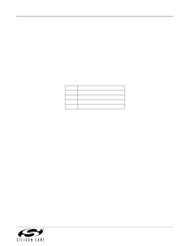
�Table� 4.� J6� Terminal� Block� Pin� Descriptions�
�Pin� #�
�1�
�2�
�3�
�4�
�Description�
�P2.5� /� AIN2.5�
�AIN2.4�
�GND� (Ground)�
�P0.0� /� Vref� (Voltage� Reference)�
�4.7.� USB� Debug� Adapter� Target� Board� Power� Connector� (J8)�
�The� USB� Debug� Adapter� includes� a� connection� to� provide� power� to� the� target� board.� This� connection� is� routed�
�from� J4[10]� to� J8[1].� Place� a� shorting� block� at� header� J8[2–3]� to� power� the� board� directly� from� an� ac/dc� power�
�adapter.� Place� a� shorting� block� at� header� J8[1–2]� to� power� the� board� from� the� USB� Debug� Adapter.� Please� note�
�that� the� second� option� is� not� supported� with� either� the� EC1� or� EC2� Serial� Adapters.�
�4.8.� Low-Pass� Filter� (J7)�
�The� C8051F310� target� board� features� a� low-pass� filter� that� may� be� connected� to� port� pin� P2.4.� Install� a� shorting�
�block� on� J7[1–2]� to� connect� the� P2.4� pin� of� the� target� device� to� the� low-pass� filter� input.� The� output� of� the� low-pass�
�filter� is� routed� to� the� PWM� signal� at� J1[2].� The� C8051F310� may� be� programmed� to� generate� a� PWM� (Pulse-Width�
�Modulated)� waveform� which� is� then� input� to� the� low-pass� filter� to� implement� a� user-controlled� PWM� digital-to-ana-�
�log� converter.� Refer� to� Applications� Note� “AN107:� Implementing� 16-Bit� PWM� Using� the� PCA”� in� the� “� documenta-�
�tion� ”� directory� on� the� CD-ROM� for� a� discussion� on� generating� a� programmable� dc� voltage� level� with� a� PWM�
�waveform� and� low-pass� filter.�
�Rev.� 0.7�
�9�
�发布紧急采购,3分钟左右您将得到回复。
相关PDF资料
C8051F320DK-U
DEV KIT FOR C8051F320/F321
C850-260-WHX
CIRCUIT PROT 260MA 850VIMP TBU
CAN0005WP
VARISTOR 18VDC 4A 0402
CB4-B0-24-650-121-C
CIRCUIT BREAKER 50A 4POLE 8 PIN
CBBJ159
TRS BULKHEAD RCPT STR PCB
CBBJ379
TRT BULKHEAD JACK STR PCB THREAD
CBBJ79
TRB BULKHEAD JACK STR PCB 3-LUG
CBBJR26
BNC BULKHEAD JACK INSUL R/A PCB
相关代理商/技术参数
C8051F310DK-T
功能描述:DEV KIT FOR C8051F310/F311 RoHS:否 类别:编程器,开发系统 >> 过时/停产零件编号 系列:- 标准包装:1 系列:- 类型:MCU 适用于相关产品:Freescale MC68HC908LJ/LK(80-QFP ZIF 插口) 所含物品:面板、缆线、软件、数据表和用户手册 其它名称:520-1035
C8051F310DK-U
功能描述:DEV KIT FOR C8051F310/F311 RoHS:否 类别:编程器,开发系统 >> 过时/停产零件编号 系列:- 标准包装:1 系列:- 类型:MCU 适用于相关产品:Freescale MC68HC908LJ/LK(80-QFP ZIF 插口) 所含物品:面板、缆线、软件、数据表和用户手册 其它名称:520-1035
C8051F310GQ
制造商:SILICONLABS 功能描述:
C8051F310-GQ
功能描述:8位微控制器 -MCU 16KB 10ADC 32P MCU RoHS:否 制造商:Silicon Labs 核心:8051 处理器系列:C8051F39x 数据总线宽度:8 bit 最大时钟频率:50 MHz 程序存储器大小:16 KB 数据 RAM 大小:1 KB 片上 ADC:Yes 工作电源电压:1.8 V to 3.6 V 工作温度范围:- 40 C to + 105 C 封装 / 箱体:QFN-20 安装风格:SMD/SMT
C8051F310-GQR
功能描述:8位微控制器 -MCU 16KB 10ADC 32Pin MCU Tape and Reel RoHS:否 制造商:Silicon Labs 核心:8051 处理器系列:C8051F39x 数据总线宽度:8 bit 最大时钟频率:50 MHz 程序存储器大小:16 KB 数据 RAM 大小:1 KB 片上 ADC:Yes 工作电源电压:1.8 V to 3.6 V 工作温度范围:- 40 C to + 105 C 封装 / 箱体:QFN-20 安装风格:SMD/SMT
C8051F310R
功能描述:8位微控制器 -MCU 10 ADC 32 Pin RoHS:否 制造商:Silicon Labs 核心:8051 处理器系列:C8051F39x 数据总线宽度:8 bit 最大时钟频率:50 MHz 程序存储器大小:16 KB 数据 RAM 大小:1 KB 片上 ADC:Yes 工作电源电压:1.8 V to 3.6 V 工作温度范围:- 40 C to + 105 C 封装 / 箱体:QFN-20 安装风格:SMD/SMT
C8051F310-TB
功能描述:插座和适配器 With C8051F310 MCU RoHS:否 制造商:Silicon Labs 产品:Adapter 用于:EM35x
C8051F310-TB-K
功能描述:BOARD PROTOTYPING W/C8051F310 制造商:silicon labs 系列:- 零件状态:在售 板类型:评估平台 类型:MCU 8-位 核心处理器:8051 操作系统:- 平台:- 配套使用产品/相关产品:C8051F31x 安装类型:固定 内容:板 标准包装:1